如果在lib檔案中 cell area的面積為 a
則在以(X_coordinate,Y_coordinate)為中心點
且邊長為√a的正方形範圍
就是此COMPONENT所佔的平面空間
任何其他的COMPONENT都不允許與這空間overlap
1. 在題目中規定BUF與DFF不得重疊,
那麼wire可否跨過BUF/DFF呢?
如果不行,
那麼也是以"面積"為範圍嗎?亦或是其座標?
ans: 我們沒有規定wire要怎麼繞
只有規定X,Y軸座標 這是用來估計wire capacitance的依據
因此沒有所謂跨不跨過的問題
只要BUF/DFF彼此不重疊即可
2. 題目中說明
total output net capacitance includes the net capacitance and the summation
of the input pin capacitances of driven cells
那麼在output檔案3中的net_load.rpt檔案中,
是上述的total output net capacitance,
還是僅有net capacitance?
ans: 這是指total output net capacitance
3. 比對ICCAD03比賽第五題,
該題之計算條件為DFF之slack必須>0
但本題中幾無提到與slack之關聯,
若僅考慮power、cell area、max clock latency,
那豈不是完全不加入BUF為最佳解??
由於測試檔案尚未release(何時會release?)
是否該條件要等測試檔案出來才會知道?
ans: 因為所有的DFF將分散於整顆CHIP
甚至會有數千數萬的DFF
因此若不加BUF
1.Clock tree 必定有DRC voilation
2.Root buffer之後的total output net capacitance
會變得非常的大 因而導致極大的功率消耗
特別注意 本題目的input clock transition time並不為0
且root buffer不能變動 跟去年明顯不同
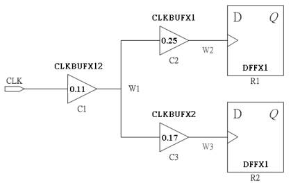
4. Can you give a example of the delay calculation? Because
The delay calculation is not specify in the content. By my
interpretation, the delay is derived by summing cell transition
and output transition of each buffer(cell) and the effect of
resistances is ignored. Is that right?
ans: No, the delay is also derived by cell input transition time and total
output capacitance.
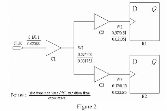
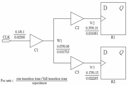
For our problem in Figure 1 and Figure 2, the cell input transition time of C1
is 0.1/0.1 (rise/fall),
the total output capacitance(net W1) is 0.031753.
So, you can use the interpolation method to calculate the rising/falling delay
of C1.
In our case,the rising/falling delay of C1 is 0.11/0.12.
5. 請問 clock buffer 是否可以 overlap 其他的standard cell ?
因為題目僅有規定clock buffer不能overlap到其他的clock buffer和 filp-flops
ans: 我們的題目僅提到DFF以及clock buffer
沒有提到一般的standard cell
將來的測試範例中也不會有任何其他的standard cell
因此這問題並不存在
6. 請問clock tree做完的結果, tree分支的部分在output檔要如何描述?
還是說要做routing描述在DEF檔中?
ans: Clock tree的結果必須 output出 design_opt.def 檔案 以及 clock_tree.v
在題目中說得很清楚
DEF檔案定義中的NET部份就可以決定所有component的連線關係
當然 , clock tree的終點必須連接所有的DFFs
7. internal power該如何計算?
在題目第8頁寫的 constant A, B, C, D 是代表什麼意思?
ans: 如同題目中對於.lib檔案的介紹
利用.lib檔中的rise_power以及fall_power groups資訊
以及cell input transition time(index_1) , total output net capacitance (index_2)
利用內插法求出A,B,C,D常數的值
因而估算出實際的internal power
A,B,C,D只是內插法中的四個常數 其值將決定internal power的結果
若真的看不懂 請詳讀Synopsys Library Compiler User Guide
其中對於Modeling Power以及Delay models的描述
8. 關於timing的計算, 能不能給個公式跟例子說明一下呢?
ans: 一樣 如上題
同樣由cell input transition time(index_1) , total output net capacitance
(index_2)來決定
只是rise_power,fall_power groups改成cell_rise以及cell_fall groups
同理 rise_transition以及 fall_transition groups則用來決定
cell output transition time 而此cell output transition time
就是後一級cell的cell input transition time
For our problem in Figure 1 and Figure 2, the cell input transition time of C1
is
0.1/0.1(rise/fall), the total output capacitance(net W1) is 0.031753.
So, you can use the interpolation method to calculate the rising/falling delay
of C1.
In our case,the rising/falling delay of C1 is 0.11/0.12.
9. 在 evaluation requirement 中提到 clock tree 必須要沒有 DRC violation.
請問在這邊是要做什麼 DRC 檢查呢?
ans: 在我們題目中 Input files的第三點有提到:
DRC constraint (i.e. the input net transition and the output net capacitance can
not be out
of the index range in .lib file).指的就是整條clock tree的所有的cell input/output
transition
time以及output net capacitance都不能超出.lib檔案中index定義的範圍
10.Does each load of a buffer have to be the same?
ans: No, the load of a buffer depends on its output net capacitance and the
summation of the input
pin capacitances of driven cells. The input pin capacitances of driven cells may
be different.
We present the cell load definition in our problem page 5, you can check it
below.
"The total output net capacitance includes the net capacitance and the summation
of the input
pin capacitances of driven cells. Assume that a CLKBUFX12 buffer drives two
DFFX1 and its output
net capacitance is 0.01pf. Then, the total output net capacitance is 0.01842pf
(0.01pf + 2 * 0.00421pf)."
11.Is evevy branching node of a clock tree a buffer? If not, how to calculate
the delay of a clock tree
without buffer?
ans: We don't consider gated clock solution for low power.
Just clock buffers and clock inverters are allowed to be used.
12.
1. 照題目上寫的 DEF 檔範例來看,所給的 DEF 檔似乎不是 standard?
舉例來說,DEF 檔裡的每個 PIN 跟 COMPONET 前面應該要有一個減號 "-"
能否改成 standard DEF file 呢?
2. 測試資料似乎還沒上網,請問何時會放上網呢? 報名快截止了
ans:
1.
其實standard DEF檔案必須包括許多其他的定義
不只是我們題目上的DEF檔案中所包括的
例如: LAYER METAL VDD VSS,還有你所說的 "-" "+" 等符號
但是在這個題目中 我們並不需要這些資訊
這些不需要的資訊 如果要通通寫進DEF檔案
我們必須對很多東西做定義與說明
這是沒有必要的
因此 我們才提出一個簡化的DEF格式
所以如果你一定要standard DEF格式
請自行轉換
2.
測試檔預計在三月份開放
13. 題目修正公告
module test(CLK);
input CLK;
CLKBUFX12 C1 (.A(CLK),.Y(W1));
CLKBUFX1 C2 (.A(W1),.Y(W2));
CLKBUFX2 C3 (.A(W1),.Y(W3));
DFFX1 R1 (.CK(W2));
DFFX1 R2 (.CK(W3));
endmodule
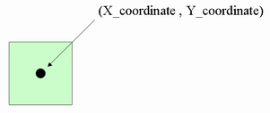
14. 請問在Def裡面所標示的COMPONENT中的座標是指這個COMPONENT的哪一個位置的點?
ans:
這是指此COMPONENT的中心點
如果在lib檔案中 cell area的面積為 a
則在以(X_coordinate,Y_coordinate)為中心點
且邊長為√a的正方形範圍
就是此COMPONENT所佔的平面空間
任何其他的COMPONENT都不允許與這空間overlap
15. wire 的 RC delay 是否不考慮,例如下圖
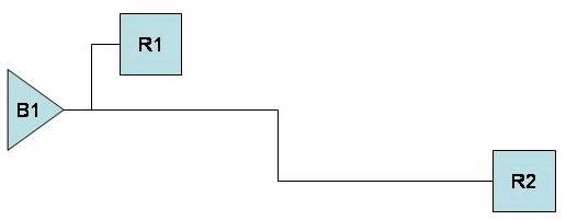
從B1 看過去 R1 ,R2 的delay 就是 B1 的cell delay
即 input transition of b1 和 c*(Dm(B1,R1)+Dm(B1,R2))+Cr1+Cr2 查表出來的cell delay
(Dm 為Manhattan distance, Cr1,Cr2 為R1,R2 的input capacitance, c 為 計算wire load的參數)
也就是說無論Dm(B1,R1)與Dm(B1,R2)相差多大,從B1 看過去兩者的delay 都是一樣的?
ans:
在non-linear delay model的運算中,並不需要wire RC delay的計算
而 input transition of b1 和 c*(Dm(B1,R1)+Dm(B1,R2))+Cr1+Cr2 查表出來的cell delay
就看做B1的delay
要計算一條clock tree之total delay
僅需計算此clock tree中所有clock buffers的delay總和
請參考Synopsys Library Compiler User Guide
其中對於non-linear delay models的描述
本題目並沒有要求計算DFF的delay
clock tree latency只計算到clock tree終點的clock buffer
如題目中的Figure 1與 Table 1
Dm(B1,R1)與Dm(B1,R2)直接影響的是B1 output net capacitance
同時也間接影響了 B1的delay與 B1的internal power,以及B1 output net 的 switching power
16. 請問output 檔案如何描述以下clock tree?
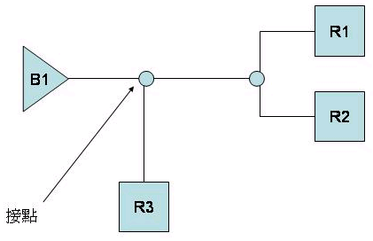
其中B1 為root ,除此之外並無其他buffer,但題目說明並無提到任何接點的表示方法,
因此此R1, R2 ,R3的delay 是否為
input transition of B1 與c*( Dm(B1,R1)+Dm(B1,R2)+Dm(B1,R3))+Cr1+Cr2+Cr3查表出來的cell
delay?
並且三個DFF的delay均相等?
ans:
input transition of B1 與c*( Dm(B1,R1)+Dm(B1,R2)+Dm(B1,R3))+Cr1+Cr2+Cr3
查表出來的cell delay 是B1的delay
如網站上Q&A第一個問題
本題目並沒有繞線的問題
所以也不存在任何接點的問題
也不要求計算任何DFF的delay
Dm(*,*) 只用來計算 net capacitance的數值
clock_tree.v 中連線的描述如下
........
B1 BUF (.A(CLK) , .Y(W1));
R1 DFF (.CK(W1));
R2 DFF (.CK(W1));
R3 DFF (.CK(W1));
.......
17. 給的.lib檔中, 最外層是不是應該要有一個library宣告:
library(library_name) {
...
...
...
}
題目上的.lib範例似乎漏掉了?
ans: 題目上的.lib只是舉例
詳細的.lib 近期會公布在網頁上
18.
(1)
請問第7頁的(5).Power report這裡
# Net 的順序需為 CLK W1 W2 W3 嗎? 或
CLK W1 W3 W2 奕可?
(2)
# Cell 的順序也是一樣要排序嗎? 或是只要列出所有的
cell 的Internal power即可?
(3)
做出圖形介面~納入加分的條件嗎
ans:
(1) 可以
(2) 列出所有cell即可
(3) 當兩組得出的power值非常接近
在 Practical issue 以及 GUI 上面若有較好的表現可能會佔優勢
然而這還是要看評分者的角度以及參考報告內容而定
19. 網頁上Q&A的第16個問題, 似乎沒有回答完全
root到R1, R2, R3的delay是否相同?
這種情況是否就zero skew?
ans:
我們沒有要求算出R1 R2 R3的delay 也沒有給定足夠的資訊
所以三個DFF是否delay相同 這是無法回答的
input transition of B1 與c*( Dm(B1,R1)+Dm(B1,R2)+Dm(B1,R3))+Cr1+Cr2+Cr3
查表出來的cell delay 是B1的delay
在non-linear model當中
由於沒有實際的 wire RC delay計算
我們不必定義root buffer 到 R1 R2 R3的delay
而 clock source 到 R1 R2 R3的clock latency
則都等於 root buffer B1 的delay(如果clock buffer只有root buffer的話)
此外 clock skew 的定義 在於兩FF之間的clock 信號差異
所以 R1<=>R2 R2<=>R3 R1<=>R3 兩兩之間的clock skew為0
Maximum clock skew 亦為0
20. cell delay 是取cell_rise delay還是cell_fall delay?
ans:
依據題目中
所有的FF都是 positive-edge-triggered flip-flops
因此你必須採用能讓FF為positive-edge-triggered的path delay
由此來決定採用cell_rise or cell_fall
21. 請問一下,在第7頁的地方 (4).cell area report中
像CLKBUFX12,CLKBUFX1..DFFX1這些cellname是固定在lib的嗎?
就是說,主辦單位的保留檔會不會有新的cellname出現?
像是多
了個CLKBUFX100 之類的來跑...
也就是想請問說所有的測試都是用同一個lib檔嗎?
包括日後的
保留檔測試..
ans:
最近會公布 lib 檔案
所有可用到的 clock buffer 以及 DFF
都包括在裡面
輸入輸出 lef 檔案 都必須與此 lib 檔案相對應
保留測試範例當然也採用同一個 lib 檔案
22. 請問有此篇問題相關的paper嗎?
好像沒有像其他篇後面有附參考文獻
ans: 沒有
23.
1.為了符合DRC role,你們必須提供由 CLK pin 腳 輸入第一顆 Buffer(root of clock tree) 的transition
time
請問,由CLK pin腳輸入第一顆 Buffer之transition time,包含rise transition time 和 fall
transition time 嗎?
還是你們只會給其中一個(例如只給rise transition time) ?
2.題目中有說到,所有的flip-flop都是positive-edge-triggered
因此, 如果我們的程式考慮 rise transition time
則 "internal power of a cell" 的算式還需算Fall_power嗎?
{ 原本公式 : internal power of cell = (Rise_power + Fall_power)*10-12*100*106 }
ans:
1. 我們會給定一個 input transition time (rise transition time = fall transition
time)
2. positive-edge-triggered flip-flop 只影響 clock latency (cell rise/fall delay)的計算
完全不影響power的計算
因為clock signal 仍有 rising/falling edge
所以clock tree中的Fall_power當然需要計算
24.
memory size有多大??
程式在跑測試檔時,系統開放給參賽者的記憶體有多大,希望主辦單位能夠說明
因為若沒有這方面的相關資訊,有時可能會造成coding中使用到相當大的記憶體
超過測試系統上提供的memory size造成程式crash,因此希望主辦單位能夠說明
ans: 2G
25.
請問input file最大可能會到多少個flip flop?
有沒有執行時間的上限呢?
ans:
對於撰寫EDA/CAD軟體來說
受限的應該是硬體(CPU,Memory)
而不是輸入條件
當然不可否認 如果無限制地給定許多FF
程式的capacity、run time 終究有其極限
但這應該由評審單位來評判
Do your best !
26.
請問是否只會用公布的測試檔測試程式?
如果會用其他保留的測試檔測試,那該檔的max skew如何定義?
ans:
在三個測試檔中 max clock skew都不是定值
因此在你的程式中
max clock skew 必須是一個輸入變數
不可寫死
27.
請問,readme中的"The clock period is always 10 ns" 是指
All clock latency 必須在 10 ns之內嗎???
ans:
不是的,clock period 為10 ns
是指 working frequency為100MHz
用來計算 power
28.
請問題目要求的是 root CLK pin 不能更動還是 root buffer 不能更動?
ans: 測試檔中CLK pin 跟 root buffer的位置是一樣的
CLK pin 與 root buffer 位置都不能變動
29.
在你們所給的題目說明文件中第六頁 net_load.rpt 檔
其中的 W1 的 pin_load 為 0.031753 如何算出
雖然你們已經告知
total output net capacitance= output net capacitance + summation of the input
pin capacitances of driven cells
且 output net capacitance = net length of all fanout 的總和
但是在 Figure 2 中及題目說明文件,都並未說明 net load 的值導出的過程
希望主辦單位可以解釋一下說明中的 W1 , W2 及 W3 如何導出的
ans:
題目中 0.031753是指 C1 的 total output net capacitance
0.031061是指 C2 的 total output net capacitance
0.022285是指 C3 的 total output net capacitance
假設C1位置為(X1,Y1) C2為(X2,Y2) C3為(X3,Y3) R1為(X4,Y4) R2為(X5,Y5)
C2的input capacitance為0.00339
C3的input capacitance為0.00338
R1 R2的input capacitance為0.00421
則
{|X1-X2| + |Y1-Y2| + |X1-X3| + |Y1-Y3|}*0.000076 + 0.00339 + 0.00338 = 0.031753
{|X2-X4| + |Y2-Y4|}*0.000076 + 0.00421 = 0.031061
{|X3-X5| + |Y3-Y5|}*0.000076 + 0.00421 = 0.022285
30. 請問max clock skew是會在那一個檔案輸入,還有輸入的格式是怎樣,因為在目前的所釋出的測試檔中都沒有看到有關max clock
skew的相關訊息
ans:
我們並不硬性規定 max clock skew 要如何輸入你的程式
或許你有GUI 或者利用其他方法
只要你的報告上有說明如何輸入 max clock skew的方法即可
另外在 clock input transition time (rise/fall) 題目皆設為0.1
因為這也是輸入條件之一
所以作法請也比照 max clock skew
31. 請問有關input格式時,我們是否需要作一個讓使用者輸入input檔名的介面,還是可以將輸入的檔名寫死(比如說讀lib檔時就讀cad_contest.lib)
ans: 不硬性規定
但報告上必須說明如何輸入
32.
1. 在測試電路中,
CLK PIN的個數會大於一個嗎?
2. Q&A 28中提到CLK pin 跟 root buffer的位置是一樣的
那不知會不會有CLK pin 的下一級有兩個或兩個以上的root buffer的情況產
生?
3. 經分析目前三個測試電路,
發現die area與dff之分佈為一「回」字形,
dff僅存在於「內部口」的範圍中,
而CLK PIN的位置也恰好在「內部口」的邊上,
那麼請教若有新增BUFFER,
可否加在「外部口」與「內部口」間之範圍呢?
ans:
1. 不會, clock pin 只有一個
2. 不會, root buffer 只有一個
3. 當然可以, 只要在 Die size的範圍內都可以擺
另外, 我們並不保證隱藏的測試範例 其DFF分佈的方式是一樣的
而且Initial clock tree , 也不保證完全沒有DRC violation
你必須確保輸出的clock tree是符合題目要求的
總之 不要因為測試範例 而對這個題目有太多的假設
33.
想請問 在此題中的 overlap 是包含 點和點 及 邊和邊的
overlap 嗎??
ex1: x1,y1 x2,y2
block a (0,0) (2,2) 邊長為 2
block b (2,2) (4,4) 邊長為 2
ex2: x1,y1 x2,y2
block a (0,0) (2,2) 邊長為 2
block b (2,0) (4,2) 邊長為 2
這2種,都算此題的overlap嗎?
ans:
題目僅規定不能overlap
這兩種都算相鄰 是合法的
34.
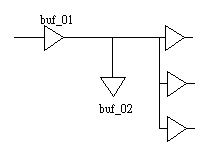
請問在此題中之buffer連接方式可否可以使用沒有fanout的buffer,如圖buf_02
若可以的話,則buf_02是否就沒有功率消耗的問題?因為buf_02的output net capacitance
為0,於library中是查不到的,或者這樣的情形有另外的算法也請告知
ans:
不行
但若你有一些新的想法
可以寫在你的報告裡面
我們會參考你的想法來斟酌加分
35.
請問evaluation priority提到:
第一是total dynamic power
第二是run time
這是否意味著power較低者分數一定比較高??
例如甲的power比乙低一些些, 但甲要跑8小時, 乙只要跑兩分鐘
而甲的分數會較高?
ans:
以出題者角度而言
基本上題目規定把 power priority 訂得比較高
是希望參賽者先往降低power結果方向來做
降低run time 為第二個考量
因為要得到好的power結果
在 Algorithm 部份勢必要多花心思
而且 Program coding時候花的 effort 較大
雖然要花較多的run time
相對而言 若在可忍受的範圍
確有其可取之處
如果程式非常快得到結果
得到power的結果僅算是普通
且報告中沒有什麼重要的結論
要得到高分就比較難
當然 這只是站在出題者的角度
實際上還要看其他評審的看法
36.
請問一下在題目的第7頁 power.rpt 檔案中
如果將 Internal power 全部加起來
C1 + C2 + C3 + R1 + R2 = 0.0950 + 0.0073 + 0.0123 + 0.0205 + 0.0194
= 0.1545
可是 power.rpt 中
The total internal power is 0.1552 mW
是有其他的 Internal power 並沒有被列出來嗎?
ans: 這是進位上的誤差 是容許的
37.
請問在report檔的部份,有些檔的輸出是小數點下兩位或者是下四位,
如skew.rpt是小數點下兩位,power.rpt是小數點下四位...,我們的輸出也是要跟題目上的位數格式一樣嗎?
假如是的話:
這樣關係到精確度問題,若兩組的結果在這些report檔因精確度問題而一樣的話,是要怎樣去評分?
不是的話:
有沒有什麼限制最多位數之類或者由使用者自己去定義輸出位數?
ans:
題目最後說明 將利用 Synopsys Power Compiler來做計算power的依據
題目上的report 檔案結果就是Power Compiler算出的結果
因此除非兩組做出同樣的clock tree
要得到同樣的power結果幾乎不可能
我們希望report 檔案格式就如同題目給定一樣 包含小數點進位
至於計算上的精確值誤差是被允許的
你的程式與Power Compiler算出來的值要能有一定程度的吻合
若有差距
題目中要求列出所有Net switching power 與 Cell internal power結果
我們將參考這結果來判定你的程式結果有無計算錯誤
評分角度題目中定義得很清楚
而且有許多測試檔來驗證各位的程式
同學不必擔心
38.
1. 對於C2 而言, 要計算出 C2 的rise output transition time 是根據 0.07 (rise input transition
time for C2)
而C2 的 fall output transition time 是根據 0.06 (fall input transition time for C2)
嗎?
還是必須根據 能讓 FF positive-edge-triggered 的path 來決定 C2 的input transition time , 例如
要計算
C2 的 rise/fall output transition time 都是用 0.07
2. 另外, 第20 題的Q & A 的有提到 cell delay的計算 , 不過還是不太清楚
若將上圖 (Figure 2) 的 C1,C2,C3 改為 inverter , 那麼相對 C1 ,C2 的input transition time 分別
採用哪組數字呢 ?
ans:
在計算clock latency上面
1.以題目為例子
所有DFF都是positive-edge triggered FF
所有C1 C2 C3的input transition time都採用rise input transition time
所以C1 C2 C3的delay都用 cell_rise table來算
W1 W2 W3的transition time亦都用 rise_transition table來算
2.若題目中 C1 C2 C3都換成 CLKINV
C1的input transition time採用rise input transition time (CLK)
C2 C3的input transition time採用fall input transition time (W1)
C1用 cell_fall table來算
C2 C3 用 cell_rise table來算
W1用 fall_transition table
W2 W3都用 rise_transition table
詳情請參考Synopsys library compiler User Guide
39.
請問是否能公布執行程式的 sun 機種
以及提供的compiler 版本,如果到時候程式寫出來了,機器卻不能跑binary
compiler 也因為不支援而無法compile,實在相當可惜。
請問下面的程式在評審的機器上面能compile嗎?
synopsys library parser - liberty parser 1.8
gcc 3.3.1 up compatible source.
ans:
SunOS 5.8 Generic_108528-23 sun4u sparc SUNW,Ultra-60 Solaris
gcc version 3.2.2
另一方面
站在出題者角度
我們不允許程式中包含任何 EDA vandor的的程式
包括你提到的 synopsys library parser - liberty parser 1.8
因為這有違公平競賽的原則
你可以用EDA工具來驗證你跑出的結果
但程式中不可以包含這些工具
40.
你好,對於第38題的回答,我還是不太不清楚,
(1) 請問,對於buffer,而言,若input net的transition要為rise,其rise transition
time是T1,則此buffer的output net的rise / fall transition time都是以T1為index來查library的rise_transitionc和fall_transition
table嗎?
或是說以input rise transition time T1來當index求output rise transition time ; input
fall transition time T2來當index求 output fall transition time?
(2)同上個問題,請問對Inverter而言, 又該如何計算呢?
(3)對inverter而言,若input net transition是Fall,則是以input Fall transition time當index 來查rise_power
table,以input Rise transition time當index查fall_power table嗎?或是Rise power和Fall
power都是以input Fall transition time來當index來查table?
ans:
1. 是以input rise transition time T1來當index求output rise transition time
input fall transition time T2來當index求 output fall transition time
請注意 問題38說明的是計算 "clock latency"
若clock tree全由 buffer組成
在計算clock latency的過程當中你將不會用到 fall transition time以及
fall_transition table
但在計算power部份
你就必須計算 fall transition time以及 fall_transition table
2. 反之 input rise transition time T1來當index求output fall transition
time
input fall transition time T2來當index求 output rise transition time
3. 沒錯 與計算 cell_delay相同
41.
我們想請教一下關於 library中index的順序. 以下表為例
index_1(input net transition time)依照題目第8頁計算內差的internal power值應為縱向的座標
但是依照常理推斷, 縱向座標應為total output net capacitance,
可以請主辦單位解釋一下這兩個index 對power的關係嗎?
rise_power(energy_template_7x7) {
index_1 ("0.0500, 0.1000, 0.4000, 0.9000, 1.4000, 2.0000, 3.0000");
index_2 ("0.00720, 0.36000, 0.72000, 1.80000, 3.24000, 4.68000, 6.12000");
values ( \
"0.3816, 0.3020, 0.2630, 0.2000, 0.1100, 0.0300, 0.0000", \
"0.4223, 0.3770, 0.3510, 0.2900, 0.2100, 0.1200, 0.0300", \
"0.5766, 0.4460, 0.4320, 0.2800, 0.1500, 0.2200, 0.1300", \
"0.8698, 0.7270, 0.6350, 0.5000, 0.4000, 0.3000, 0.2100", \
"1.1520, 0.9620, 0.8730, 0.7600, 0.6600, 0.5600, 0.4700", \
"1.4930, 1.2510, 1.1860, 1.0100, 0.9000, 0.8000, 0.7000", \
"2.0370, 1.7380, 1.6560, 1.4500, 1.3100, 1.2000, 1.1000");
}
ans:
題目定義的沒錯
這是Synopsys liberty library standard
如果 input transition time 為 0.1 定值
你用到的 rise_power 值應為
"0.4223, 0.3770, 0.3510, 0.2900, 0.2100, 0.1200, 0.0300"
42.
請問..程式執行的時間有規定上限的時間嗎?
CLK_10000.def,若執行了,3,4個小時,仍在接受範圍之內嗎?
ans:
如果你的程式可能會跑很久
請在報告中註明你預計的 run time
我們會在時間許可之下儘可能進行驗證
43.
請問在輸出檔案 skew_rpt 中,
有一行為
# Maxiumn clock skew
R1 R2 0.08
以上R1、R2為範例Fig. 2中之DFF
因為只有兩個DFF所以可以一行解決,
那若max latency的dff大於一個
min latency的dff也大於一個
那在這行中是要寫出所有的排列組合?
還是只要寫出其中任一個dff即可?
ans: 列出一組DFF 即可
但 maximum clock skew 值不可有錯
44.
Q&A 39 得知,不得使用synopsys library parser - liberty parser 1.8
這造成我們對.lib讀檔動作相當麻煩..
請問如果做此限制的話,我們是否能將.lib的table直接寫死在程式裡呢?
(因為從頭到尾都是用同一個.lib檔...)
ans:
針對此競賽問題 這樣做雖然沒有問題
但在Pratical issue的考量上
市面上沒有任何 EDA tool只允許讀入一種library
此作法並不符合EDA工具發展的精神
45.
是否禁止使用任何open source的library?
例如一些GUI的library, 數值運算的library (GNU Scientific Library)
ans:
並不禁止使用open source的library.
但是在繳交程式時, 請將相關的library及設定先行設好.
在測程式時有任何編譯上的問題請自行承擔.
46.
請問:如問題26,clock skew constraint不能寫死要由變數去控制;那如此問題27中的clock period是不是也不能寫死,由變數控制計算power,亦或永遠都是10ns?因為公怖的所有測試檔都是10ns
ans:
在求power的過程中
clock period 僅是一個固定的常數
也就是說
total power與clock frequency成正比
因此將clock period設為變數是沒意義的
47.
請問:在net_load.rpt檔中記錄所有net的capacitance,但是題目的範例中只有記錄
W1、W2、W3三個net capacitance,沒有記錄到CLK到C1間的net capacitance。
是不是因為問題28中講到CLK跟C1是一樣的位置,所以沒有net,不考慮寫到net_load.rpt?但是在design.def中似乎有存在一個CLK的net到C1去,則此capacitance
到底要不要寫到net_load.rpt去?還是因為這個capacitance是固定的,所以才不寫到檔案中?
ans:
我們把 clock pin 位置與 root buffer重疊
意思就是 CLK 的 wire capacitance
僅由 C1 的 input pin capacitance (0.02588)所組成
由此來計算 CLK 的 switching power
如題目規定 是可以不用列出 CLK 的 net load
48.
主辦單位所提供的測試檔
在某些句子的最後結尾會有個不必要的空格
請問是"必要的"還是說可以自行刪除??
ans: 空格應該不影響程式對資料的讀取,
請自行解決此問題。
49. [通告]
主辦單位已經將郵寄報告以及FTP上傳作品的方式公布於參賽手冊(April 22, 2004版本), 敬請盡速至競賽網頁下載. 另外,
FTP站也已開放上傳作品, 也請盡速確認能否成功登入.
若有任何疑問, 請來信 cad@cs.nthu.edu.tw
謝謝
50.
請問Q&A 第40題第3小題的回答:
" 對inverter而言,若input net transition是Fall,則是以input Fall transition
time當index 來查rise_power table,以input Rise transition time當index查
fall_power table嗎? "
是這句沒錯??
還是
" 或是Rise power和Fall power都是以input Fall transition time來當index來查
table? "
這句沒錯??
ans:
對inverter而言,若input net transition是Fall,則是以input Fall transition time
當index 來查rise_power table,以input Rise transition time當index查fall_power
table
與計算 cell_delay方式相同